


Download PDF

IBM and Cadence: Streamlining Mainframe Computer Designs with Complex PCB Systems
Technology Category
- Processors & Edge Intelligence - Microcontrollers & Printed Circuit Boards
- Sensors - Temperature Sensors
Applicable Functions
- Product Research & Development
Use Cases
- Manufacturing Process Simulation
- Time Sensitive Networking
Services
- Hardware Design & Engineering Services
- System Integration
The Challenge
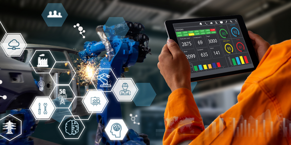
IBM, a leader in mainframe computing, was facing challenges in designing highly complex printed circuit boards (PCBs) for their mainframe computers. These PCBs, measuring as large as 50cm x 60cm, carry tens of thousands of signal interconnects in more than 10 layers of circuitry, with pin counts reaching 5,000 per component and more than 5,000 connections at the board level. The complexity of these designs made traditional schematics cumbersome and time-consuming to work with and analyze. IBM attempted to simplify the process by developing a solution based on entering the design attributes of each signal in a table or spreadsheet format. However, this added another step in the process as engineers had to convert the information into Hardware Description Language (HDL) to interface with the design platform. Additionally, analog elements could not be treated in this way and had to be configured manually.
About The Customer
IBM has been a leading player in mainframe computing for over 50 years. The company is known for its large-scale designs, creating mainframe computers that employ highly complex printed circuit boards (PCBs). These PCBs are enormous configurations of super-miniaturized components, with a single board carrying tens of thousands of signal interconnects in more than 10 layers of circuitry. The complexity of these designs, with pin counts reaching 5,000 per component and more than 5,000 connections at the board level, presents significant design challenges. Despite these challenges, IBM continues to innovate and lead the way in mainframe computing.
The Solution
IBM R&D Lab Germany adopted Cadence's Allegro System Architect GXL, an integrated solution that managed both tabular and schematic data in a full design and simulation environment. This solution allowed designers to enter and manipulate signal specifications as easily as with an accounting spreadsheet, reducing the input time to one-tenth of the time required to work directly with schematics, and with fewer errors. The solution also enabled rapid compilations, reducing the design code compilation time from 8-10 hours to a matter of seconds. This allowed for quick detection of errors and increased efficiency and productivity. The integrated environment of Allegro System Architect GXL also allowed engineers to assess more quickly and easily how front-end definitions would affect back-end design issues, reducing the time required for PCB development by 80%.
Operational Impact
Quantitative Benefit
Related Case Studies.
Case Study
Battery manufacturer Industrial Digital Twin
For optimum control of product quality, Banner relies on a high production depth. Its 560 production employees produce nearly all the components in¬-house that they need to make finished batteries on Banner’s six assembly lines. This includes the plastic parts for the battery cases as well as the paste-filled lead oxide grids. Their production involves two to five¬ days rest in maturing chambers to create optimum current absorption and storage capacity. Banner’s ongoing success was accompanied by a continuous, organic growth of the production facilities, adding or extending hall after hall until the complex filled the site that had seemed ever so spacious when the company moved here from a smaller place in 1959. These developments led to a heterogeneous production environment. “This confronts us with significant challenges, particularly concerning intra¬logistics issues, such as scheduling for the maturing chambers,” says Franz Dorninger, technical director at Banner. “We contemplated various ways to overcome this problem, including relocating to new premises.”

Case Study
Centralizing Data for Improved Efficiency: A Case Study on Malvern Panalytical
Malvern Panalytical, a UK-based hi-tech electronics company, was grappling with the challenge of decentralized data storage. The company had a vast amount of unstructured data scattered across various platforms, from hard drives to emails and floppy disks. This made the data searching process extremely cumbersome and inefficient. The company's rapid growth, from 200 to over 1,000 employees in a decade, and expansion across three continents further exacerbated the need for a more structured and centralized data system. As a company involved in electronics manufacturing and software development, it was crucial for Malvern Panalytical to find a platform that could structure all their data, track all modifications of documents in real time, and provide clear visibility of the internal information flow across all its facilities.
Case Study
Managed Hosting Platform
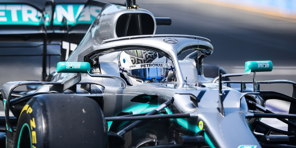
Formula 1® is a sport where every millisecond matters. With changing preferences and the growth of the digital medium, many fans choose to experience the sport through the F1.com website. The website needs to deliver a superior experience to tens of millions of fans across the world consistently. Hence, it is imperative to have a robust platform that can deliver the required performance and scale with growing trac and dynamic fan expectations. Some of the key challenges are: • Every race weekend, Formula1.com attracts up to 7 million fans. Managing this huge surge in website traffic, requires a scalable hosting platform that can simultaneously allow millions of fans to experience the excitement of the sport seamlessly. • Fans across the globe expect an engaging and immersive experience through enriched and enhanced race content across multiple devices. To meet this requirement Formula1.com needs to have a robust platform that is able to deliver real-time updates and information across screens, be it tablets, TVs or smartphones. • A global brand like Formula 1® needs to ensure it delivers a consistent user experience across all platforms across the globe. This consistent delivery of enriched content cannot be compromised through downtime or any other issue at any point. • In an age where threats to global websites are prevalent, Formula 1® needed a platform that was ready to meet any challenge to its website. They needed a solution that delivers consistency, scalability and yet at the same time is continuously monitored, secure and reliable.
Case Study
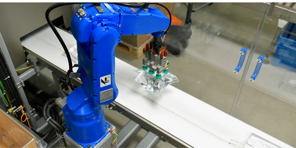
Flow Robotics: Scaling Up Production and Accelerating Product Development with IoT
Flow Robotics, a Danish manufacturer, developed flowbot™ ONE pipetting robots to alleviate the strain on bioanalysts in life-science laboratories and hospitals across Europe. These robots were designed to automate part of the testing process, speeding up the time it takes to produce results and reducing pressure on staff. However, the company faced challenges in scaling up production and accelerating product development. High workloads and physically challenging conditions have long been an issue for laboratory professionals. Flow Robotics estimates that around half of medical lab technicians carry out the same arm movements for at least a quarter of their working day. The American Society for Clinical Pathology reported that 85% of laboratory professionals feel burnt out; 36% struggle with inadequate staffing; and 32% face a heavy workload and pressure to complete all testing on time.

Case Study
EDF's Transformation: Enhancing Employee Experience through IT Modernization
EDF, a major UK utilities company, was grappling with a highly customized service management system that was largely manual, with limited potential for automation. This made it difficult to predict or prevent system failures and provide a resilient service. The company's IT system for incident handling was purely manual, leaving no room for modernization. EDF wanted to serve its business and residential customers better by improving the response time to rising energy demands. To achieve this, the company needed to provide its employees with the right tools for improved productivity, better collaboration, and an enhanced IT experience at a reduced cost to serve.
