


Download PDF

NVIDIA and Cadence: Streamlining PCB Design with IoT
Technology Category
- Processors & Edge Intelligence - Microcontrollers & Printed Circuit Boards
- Sensors - Liquid Detection Sensors
Applicable Industries
- Electronics
- Equipment & Machinery
Applicable Functions
- Product Research & Development
Use Cases
- Additive Manufacturing
- Time Sensitive Networking
Services
- Hardware Design & Engineering Services
The Challenge
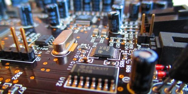
NVIDIA, a leading company in visual computing technologies, was facing a significant challenge in meeting the stringent time-to-market windows for its high-performance gadgets. The company's average design cycle was less than six months, from silicon tapeout to printed circuit boards (PCBs) ready for the marketplace. NVIDIA design teams were using Cadence tools to create their IC package and board designs. They had also developed several in-house tools for ball grid array (BGA) fanout and routing to augment their existing Cadence® Allegro® constraint-driven PCB design flow. However, the pressures of product miniaturization and high-density interconnect (HDI), combined with an increasing number of constraints, was creating new challenges. The question was whether to invest time and resources developing tools to enable HDI, or to adopt a new solution. And since NVIDIA was designing with high-speed constraints but also using “build-up” technology to handle BGA fanout, they would need a highly flexible solution that could address both sets of requirements.
About The Customer
NVIDIA is a leading company in the development of visual computing technologies. It is the inventor of the GPU, a high-performance processor that generates breathtaking, interactive graphics on personal computers, game consoles, and mobile devices such as smartphones. To keep up with consumer demand for such high-performance gadgets, NVIDIA must meet stringent time-to-market windows. The company’s average design cycle is less than six months, from silicon tapeout to printed circuit boards (PCBs) ready for the marketplace. NVIDIA design teams were using Cadence tools to create their IC package and board designs.
The Solution
NVIDIA decided to migrate to the latest Allegro PCB Design technologies, which―starting with the 16.2 release―enable a constraint-driven HDI design flow. The new Cadence flow combines the proven Allegro constraint-driven PCB design flow with a comprehensive set of automation-assisted manufacturing rules for all different styles of HDI designs, from a hybrid build-up/core combination to a complete build-up process. Allegro PCB Editor now includes automation for adding and managing micro vias to shorten the time to create designs that are correct-by-construction. From front-end design creation to signal integrity to back-end layout, the Allegro 16.2 release boosts productivity and predictability while streamlining the product development cycle. The Cadence solution automatically drops the vias in the correct location, which greatly increases efficiency and eliminates previous user-developed and user-maintained workarounds. Now that the NVIDIA team has an integrated HDI design and validation mechanism, they don’t have to spend time building internal automation tools or performing post-processing.
Operational Impact
Quantitative Benefit
Related Case Studies.

Case Study
Smart Water Filtration Systems
Before working with Ayla Networks, Ozner was already using cloud connectivity to identify and solve water-filtration system malfunctions as well as to monitor filter cartridges for replacements.But, in June 2015, Ozner executives talked with Ayla about how the company might further improve its water systems with IoT technology. They liked what they heard from Ayla, but the executives needed to be sure that Ayla’s Agile IoT Platform provided the security and reliability Ozner required.

Case Study
IoT enabled Fleet Management with MindSphere
In view of growing competition, Gämmerler had a strong need to remain competitive via process optimization, reliability and gentle handling of printed products, even at highest press speeds. In addition, a digitalization initiative also included developing a key differentiation via data-driven services offers.

Case Study
Remote Temperature Monitoring of Perishable Goods Saves Money
RMONI was facing temperature monitoring challenges in a cold chain business. A cold chain must be established and maintained to ensure goods have been properly refrigerated during every step of the process, making temperature monitoring a critical business function. Manual registration practice can be very costly, labor intensive and prone to mistakes.
Case Study
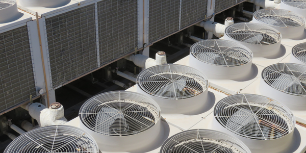
Predictive Maintenance for Industrial Chillers
For global leaders in the industrial chiller manufacturing, reliability of the entire production process is of the utmost importance. Chillers are refrigeration systems that produce ice water to provide cooling for a process or industrial application. One of those leaders sought a way to respond to asset performance issues, even before they occur. The intelligence to guarantee maximum reliability of cooling devices is embedded (pre-alarming). A pre-alarming phase means that the cooling device still works, but symptoms may appear, telling manufacturers that a failure is likely to occur in the near future. Chillers who are not internet connected at that moment, provide little insight in this pre-alarming phase.
Case Study
Premium Appliance Producer Innovates with Internet of Everything
Sub-Zero faced the largest product launch in the company’s history:It wanted to launch 60 new products as scheduled while simultaneously opening a new “greenfield” production facility, yet still adhering to stringent quality requirements and manage issues from new supply-chain partners. A the same time, it wanted to increase staff productivity time and collaboration while reducing travel and costs.
