


下载PDF

Zyvex Corporation: Pioneering 3D MEMS Technology for Nanotech Applications
技术
- 传感器 - 加速度计
- 传感器 - 声学传感器
适用行业
- 电子产品
- 设备与机械
适用功能
- 产品研发
用例
- 网状网络
- 虚拟原型与产品测试
服务
- 硬件设计与工程服务
- 系统集成
挑战
Zyvex Corporation 是一家领先的分子纳米技术开发公司,面临着开发微机电系统 (MEMS) 技术以实现新纳米技术应用的挑战。大多数商用 MEMS 器件本质上是二维的,生长在平坦的基底上或从平坦的基底上蚀刻而成。然而,Zyvex 看到了 MEMS 技术的潜力,该技术可以提供具有 3D 特性的结构和设备。挑战在于制造过程。构建 3D MEMS 设备需要某种形式的组装,以将结构从制造平面升起并将其移动到适当的位置。传统的组装方法成本高昂,而替代方法也有局限性。此外,计算分析的使用对于微结构的设计至关重要,因为微加工周期可能需要长达四个月的时间。
关于客户
Zyvex Corporation 总部位于德克萨斯州理查森,是第一家分子纳米技术开发公司,也是商业纳米技术应用的积极开发商。该公司拥有材料、工具和结构三大产品线,专注于三个细分市场:航空航天和国防;医疗保健和医学;以及电子和半导体。 Zyvex 客户包括波音、Easton Sports、霍尼韦尔国际和德州仪器等行业领导者。该公司在州和联邦机构的资助下活跃于多个研究领域。
解决方案
Zyvex 公司开发了一种独特的方法来克服这些挑战。他们设计了兼容的 MEMS 组件,这些组件可以在自动化过程中解开、从晶圆平面上移除并组装。这是通过使用 MEMS 末端执行器和高精度机器人技术的定向拾放微组装工艺实现的。这使得集成在单独工艺中制造的微型元件成为可能。 Zyvex 在 MEMS 设计过程中也严重依赖有限元分析 (FEA) 工具。这些工具使他们能够设计、分析和测试 MEMS 结构,从而显着加快工作速度。他们使用 Altair HyperMesh 等先进的 FEA 工具来更好地控制网格密度,并使用 Altair HyperView 等后处理工具的可视化功能来了解 MEMS 设备的性能和功能。
运营影响
数量效益
相关案例.
Case Study
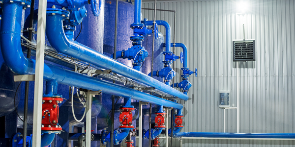
Smart Water Filtration Systems
Before working with Ayla Networks, Ozner was already using cloud connectivity to identify and solve water-filtration system malfunctions as well as to monitor filter cartridges for replacements.But, in June 2015, Ozner executives talked with Ayla about how the company might further improve its water systems with IoT technology. They liked what they heard from Ayla, but the executives needed to be sure that Ayla’s Agile IoT Platform provided the security and reliability Ozner required.


Case Study
IoT enabled Fleet Management with MindSphere
In view of growing competition, Gämmerler had a strong need to remain competitive via process optimization, reliability and gentle handling of printed products, even at highest press speeds. In addition, a digitalization initiative also included developing a key differentiation via data-driven services offers.

Case Study
Remote Temperature Monitoring of Perishable Goods Saves Money
RMONI was facing temperature monitoring challenges in a cold chain business. A cold chain must be established and maintained to ensure goods have been properly refrigerated during every step of the process, making temperature monitoring a critical business function. Manual registration practice can be very costly, labor intensive and prone to mistakes.
Case Study
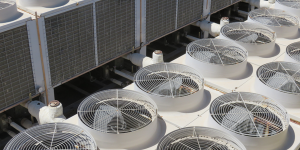
Predictive Maintenance for Industrial Chillers
For global leaders in the industrial chiller manufacturing, reliability of the entire production process is of the utmost importance. Chillers are refrigeration systems that produce ice water to provide cooling for a process or industrial application. One of those leaders sought a way to respond to asset performance issues, even before they occur. The intelligence to guarantee maximum reliability of cooling devices is embedded (pre-alarming). A pre-alarming phase means that the cooling device still works, but symptoms may appear, telling manufacturers that a failure is likely to occur in the near future. Chillers who are not internet connected at that moment, provide little insight in this pre-alarming phase.
Case Study
Premium Appliance Producer Innovates with Internet of Everything
Sub-Zero faced the largest product launch in the company’s history:It wanted to launch 60 new products as scheduled while simultaneously opening a new “greenfield” production facility, yet still adhering to stringent quality requirements and manage issues from new supply-chain partners. A the same time, it wanted to increase staff productivity time and collaboration while reducing travel and costs.
